
Today, the Intel Foundry Technology Research team announced technology breakthroughs in 2D transistor technology using beyond-silicon materials, chip interconnects, and packaging technology, among others. The company will unveil its research in seven of its own papers, along with two more papers in collaboration with industry partners like imec, at the IEEE International Electron Devices Meeting (IEDM) 2024 conference.
Intel’s disclosures include new research that enhances gate-all-around (GAA) transistor scaling and performance both with silicon and with atomically-thin 2D transistors that use beyond-silicon materials. Intel also outlined its subtractive Ruthenium technology that improves interconnect performance and scalability, ultimately enabling smaller wires between transistors, and a chip packaging breakthrough that improves chip-to-chip assembly throughput by 100x.
Intel’s Technology Research team, formerly known as the Components Research team for the last 50 years, is part of Intel Foundry. This team works on developing products intended for commercialization in the nearer term than the more far-looking initiatives at Intel Labs. The Technology Research team is known for paving the way for many of Intel’s fundamental technologies, with the latest innovations like the PowerVia backside power delivery and RibbonFET gate-all-around architecture originating in this group.
Intel hasn’t presented the papers at IEDM yet, and our one-on-one discussion with the General Manager of the Research Team isn’t until tomorrow. We’ll provide the descriptions of the breakthroughs below, but we’ll circle back with an update to fill in more details.
Interconnect scaling breakthough
As transistors get smaller, so too must the wires (interconnects) that connect them. Copper is the material of choice for the billions of nanometer-scale wires that move power and data around inside the chip in a complex 3D grid (you can see what this looks like in this video). In fact, up to 50 miles of interconnect wiring are inside modern chips. However, the ability to shrink these microscopic wires is running out of steam, and most alternatives aren’t suitable for high-volume manufacturing. This is a critical roadblock to moving forward to smaller process nodes.

Much like a standard copper wire you use in your home for electrical devices, the wires that carry electrons between transistors need an insulator, in this case, a dielectric coating, to prevent the electrons from going places they shouldn’t. However, the wires also require a barrier to prevent copper diffusion that could contaminate the dielectric. This barrier creates issues with shrinking the wires.
Shrinking the interconnect wires in a processor is exceedingly difficult because of the requirements of copper damascene, an additive process used to create the wires. First, a trench is created, then a barrier is deposited in the trench on top of a dielectric. A seed layer is then placed on top of the barrier to enable copper electroplating; then, copper is deposited on top. Any excess material at the top is then polished away.
As shown in the image above, decreasing the amount of copper helps to thin the wire, but it also decreases the ratio of the copper (bulk) to the barrier and seed layer, and resistivity increases exponentially as the wires are shrunk. This means the wires carry less current, slowing the device speed (among other effects) and impacting capacitance.
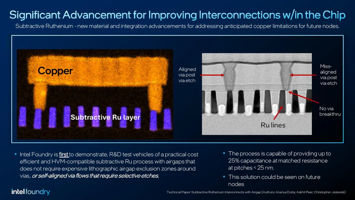
Intel’s Technology Research team has developed a process suitable for high-volume manufacturing that uses Ruthenium instead of copper. It also features air gaps.
Air gaps are a technology that Intel introduced back in the 14nm process node. This technique removes sections of the insulative dielectric, leaving air instead (air has a dielectric constant of around 1.0) to reduce capacitance (Intel claimed a 17% improvement in capacitance with 14nm).
Intel hasn’t shared the deep dive details of its Subtractive Ruthenium process, but we’re sure to learn more details during the presentation. Intel says its Subtractive Ruthenium process with airgaps provides up to 25% capacitance at matched resistance at sub-25nm pitches (the center-to-center distance between interconnect lines). Intel says its research team “was first to demonstrate, in R&D test vehicles, a practical, cost-efficient and high-volume manufacturing compatible subtractive Ru integrated process with airgaps that does not require expensive lithographic airgap exclusion zones around vias, or self-aligned via flows that require selective etches.”

Intel envisions using this technique for the most critical layers with the smallest pitches at first, while standard copper damascene will be used for the larger upper layers. Naturally, Rutheniuem will also be beneficial for its PowerVia backside power delivery. In the end, these smaller wires will enable connecting to smaller transistors, and Intel says this tech will likely be used in future Intel Foundry nodes.
Gate-All-Around (GAA) transistor breakthroughs


Intel’s RibbonFET is its first new transistor design since FinFET arrived more than 13 years ago. It is Intel’s first gate-all-around (GAA) transistor, debuting with the 20A and 18A nodes. It features stacked nanosheets surrounded entirely by a gate, as opposed to the fins surrounded on three sides used for FinFET.


Now, the challenge is to shrink the GAA designs further, and Intel is tackling that in both standard silicon designs and using new 2D materials. With standard silicon, Intel’s transistor disclosures show enhanced gate-all-around RibbonFET CMOS scaling, resulting in a gate length of 6nm and a nanoribbon/nanosheet thickness of 1.7nm while delivering improved short channel effects and higher performance.
On the first side, the gate length vs electron velocity graph on the right shows an impressive profile. The table in the center of the slide shows comparisons to existing transistor technologies, with the Tfin/Tsi (fin thickness/nanoribbon thickness) for the nanoribbon being nearly twice as thin as the fin used in FinFET.
The biggest question is, what’s next after silicon? After CFET transistors arrive, the next step of GAA is to change the materials used in NMOS and PMOS transistors to 2D materials (only a few atoms thick). The second slide outlines Intel's advances using atomically thin transition-metal dichalcogenide (TMD) materials, widely thought to be the materials used after silicon.
Intel fabricated 2D gate-all-around NMOS and PMOS transistors with a gate length of 30nm using moly-based material. Intel claims this effort delivered ‘best in class NMOS drive currents,’ a 2X improvement over the next-best published result. The chart on the right shows the research vehicle outperforming other such exploratory efforts into TMDs.
Intel’s transistor track also includes a view back at the last 60 years of transistor tech and a call to action for the industry to develop transistors that operate at ultra-low Vdd (supply voltages) of sub-300mV, a substantial decrease from today’s 1V range. This is a stretch goal for the 2030s and 2040s.
Packaging breakthroughs

Intel's new Selective Layer Transfer (SLT) tech enables attaching an entire wafer of chip dies to another wafer at extremely high speeds —Intel says SLT enables a 100X increase in throughput for the chip-to-chip assembly process. With SLT, the entire wafer full of dies can be connected to the underlying wafer at once, and individual dies can be selected for bonding while others can be excluded. This tech uses inorganic infrared laser debonding.
Intel also cites that SLT "enables ultra-thin chiplets with much better flexibility to enable smaller die sizes and higher aspect ratios versus traditional chip-to-wafer bonding." Intel's descriptions of this new tech aren't entirely clear, so we hope to learn more from the presentation. It appears this would be a great alternative to approaches that use reconstituted wafers. We'll add more detail here once we learn more.

Intel will also have an IEDM-invited talk about tomorrow's packaging solutions. This slide above revealed EMIB-T, which hasn't been disclosed previously. As a reminder, EMIB is Intel's Embedded Multi-Die Interconnect Bridge, a low-latency, low-power, and high-bandwidth interconnect that connects die together.
Intel disclosed that EMIB-T stands for EMIB-TSV. This variant marks the first EMIB implementation that uses TSVs to send the signal through the bridge with TSVs instead of wrapping the signal around the bridge.


At IEDM, Intel will submit seven papers along with two other papers with partners such as imec, Aixtron, and the Tor Vergata University of Rome.
We have time carved out with Intel for follow-up questions, and we'll update this piece with more details soon.


